當(dāng)前位置:首頁 > 產(chǎn)品中心 > 二維材料 > 二維材料薄膜 > 機(jī)械剝離單層二硫化鎢薄膜


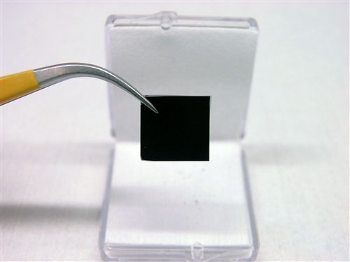
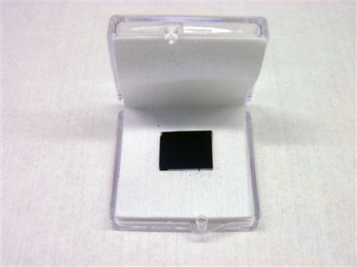
簡要描述:Monolayer tungsten disulfide (1H-WS?) flakes have been exfoliated from bulk tungsten disulfide (2H-WS?) onto 90nm thermal oxide and measures from 5micron up to 40micron in size.
 產(chǎn)品型號(hào):
  廠商性質(zhì):生產(chǎn)廠家
 更新時(shí)間:2024-06-03
 訪 問 量:853
相關(guān)文章
Related Articles詳細(xì)介紹
Monolayer tungsten disulfide (1H-WS?) flakes have been exfoliated from bulk tungsten disulfide (2H-WS?) onto 90nm thermal oxide and measures from 5micron up to 40micron in size. Each sample contains at least one single-layer WS? and is easy to find with the given x and y coordinates. Full characterization is performed on each monolayer flake. Typically, single-layer WS? show strong PL at 2.02eV with 0.04 to 0.08eV FWHM, All the data is provided with the sample and data includes Raman, photoluminescence, 100x optical images, and x,y coordinates.
Photoluminescence (PL): In the single layer form, tungsten diselenide possesses direct band-gap at 2.02eV. PL measurements show strong PL peak located at 2.02V with 0.04-0.08 eV PL FWHM.
Optical Microscope images: Each sample is inspected under the optical microscope and x-y coordinates are recorded.
Contact us for more information
Possible applications:
Electronics
Sensors - detectors
Optics
STM - AFM applications
Molecular detection - binding
Ultra-low friction studies
Materials science and semiconductor research


產(chǎn)品咨詢
聯(lián)系我們
上海巨納科技有限公司 公司地址:上海市虹口區(qū)寶山路778號(hào)海倫國際大廈5樓 技術(shù)支持:化工儀器網(wǎng)掃一掃 更多精彩

微信二維碼

網(wǎng)站二維碼